I am an electronic engineering student at the Simon Bolivar University in Venezuela (USB), a few months ago I was studying the subject "Electronic devices" where we were evaluated in the design of a NAND gate using the "Electric" program, earlier in other subject we had Studied how the logic gates were composed, however the objective of this class was to investigate more about its inner workings.
The schematic assembly of the NAND gate in "Electric" was made to be used as a guide:
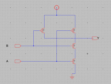
Own image
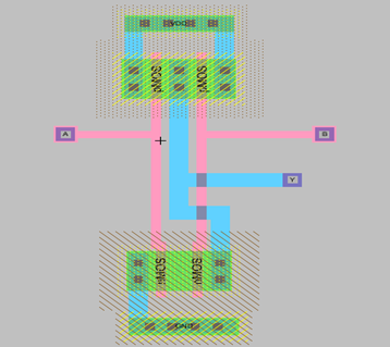
The layout corresponding to a NAND gate was assembled.
As required by the design, two NMOS transistors and two PMOS transistors with width 12 and length of 2 were used, connected with active N and P metal plates respectively of equal measures, all rotated 90 degrees, following the respective schematic, the N and P, keeping the distances between them to avoid distance errors when connected. They were joined by type 1 metal and poly silicone, to obtain the desired design:
Own image
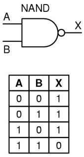
We know the truth table of the NAND gate:
Fuente
As it is the negation of the AND gate, when both inputs are pulse zero, or both are different, a pulse one will be reflected in the output, but when both inputs are a pulse one, a pulse zero will be reflected in the output. This data was used to simulate the gate in the LTSPICE and to design the NAND gate.
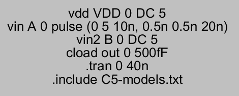
The parameters for the code were defined in SPICE where it was set:
Own image
The VDD variable as the source of the circuit with a value of 5V DC.
Vin A as a pulse train between 0 and 5V with initial delay of 10nseg, a fall and rise time of 0.5nseg and a period of 20nseg. For a simulation time of 20nseg.
To all this was added the C5-models file that contains a library with the SPICE model of the transistors.
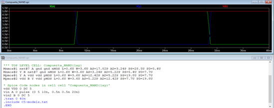
Having in the graphs:
Input A: Green.
Input B: Red.
Output Y: Blue.
The inputs were chosen in this way to always have a pulse one present at input B, which is read as the 5V input, while input A will vary thanks to the pulse train so it will change input from 0 to 1. Thanks to the initial delay of the pulse train, input A will start at 0V, and since input B is always at 5V, they mean inputs of 0 and 1, therefore output 1 equal to 5V, will be observed at the output, as seen In the NAND truth table, when 10nseg has elapsed, input A will change to 1, that is, 5V, therefore we will be in the presence of two inputs 1, that is, 5V. Therefore, the gate output will be 0, that is, 0V. After another 20sec, input A will change again and therefore the output will see the 5V voltage again.
Own image
This shows that output 1 is obtained, for the cases in which the inputs are 0 and 1, as well as the only case where output 0 is obtained, which is when both inputs are 1.
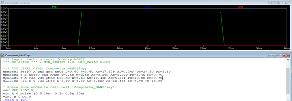
Below is the case where input B is always 0, that is 0V, so the value of input A does not matter, a 1 will always be observed at the output.

Own image
And we get:
Own image
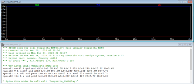
Below is the case for both inputs 0, where it will be observed that the output will always be 1, that is, 5V.

Own image
Own image
In this way, all cases of the two-input NAND gate are demonstrated, so the assembly performed in "Electric" and simulated in the LTSPICE works correctly.
Source
Copying and pasting previous posts or significant parts there of could be seen as spam when:
Spam is discouraged by the community and may result in the account being Blacklisted.
Please refrain from copying and pasting previous posts going forward. If you believe this comment is in error, please contact us in #appeals in Discord.
Thanks for sharing your creative and inspirational post on HIVE!
This post got curated by our fellow curator @tibfox and you received a 100% upvote from our non-profit curation service!
Join the official DIYHub community on HIVE and show us more of your amazing work!
Saludos @orbital753 puedes usar la etiqueta #stem-espanol y #stemsocial para una mejor visualizacion de tus publicaciones
Muchas gracias @carloserp-2000 .
Saludos.
Thanks for your contribution to the STEMsocial community. Feel free to join us on discord to get to know the rest of us!
Please consider supporting our funding proposal, approving our witness (@stem.witness) or delegating to the @stemsocial account (for some ROI).
Please consider using the STEMsocial app app and including @stemsocial as a beneficiary to get a stronger support.
Congratulations @orbital753! You have completed the following achievement on the Hive blockchain and have been rewarded with new badge(s) :
You can view your badges on your board And compare to others on the Ranking
If you no longer want to receive notifications, reply to this comment with the word
STOPDo not miss the last post from @hivebuzz:
Support the HiveBuzz project. Vote for our proposal!