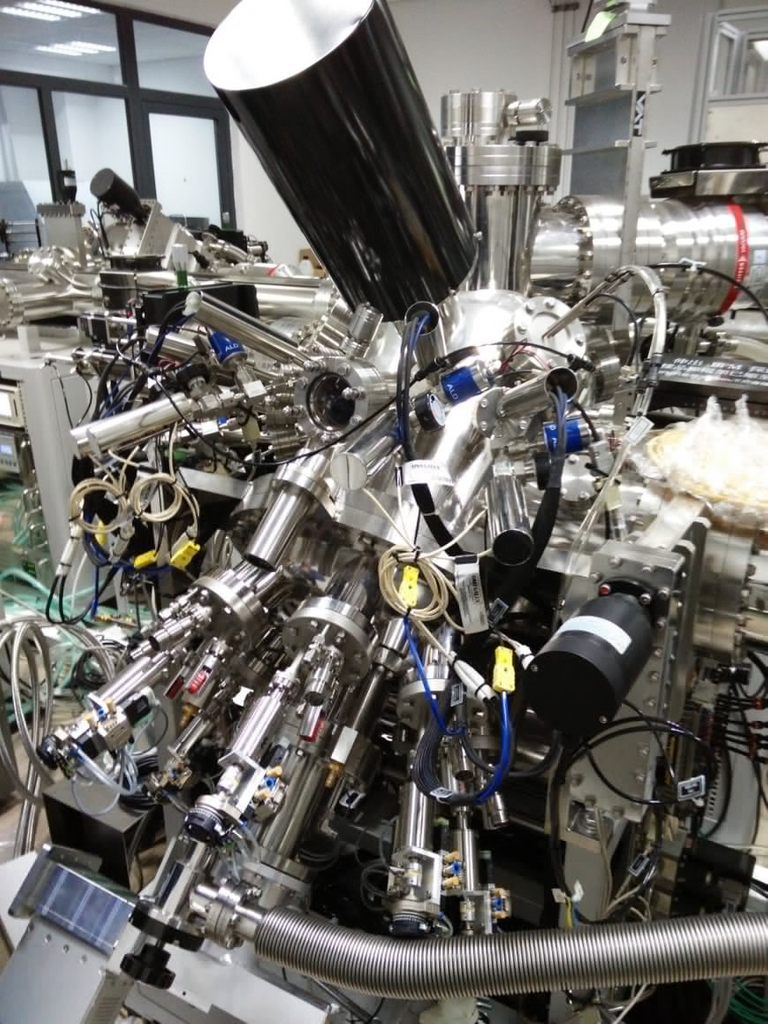
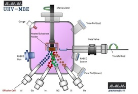
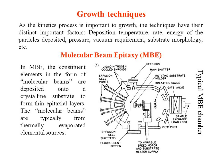
The word epitaxy comes from the Greek is a combination of two words epi (top) and taxi (arranged). Molecular Beam Epitaxy (MBE) or Epitaxy Flow Molecule is a process of epitaxial growth involving the reaction of atomic routines with crystalline surfaces in extremely high vacuum (UHV) conditions.
. Clean substrate surface
. Precisely temperature control of evaporation material
. In-situ coating monitoring by RHEED system
. Layer by layer deposition (epitaxy). source
In superconductors, the resistance drops suddenly when it becomes zero when the material is cooled below the critical temperature. The electric current flowing in the superconducting wire loop can survive indefinitely without a power source. Superconductors require very cold temperatures, on the order of 39 kelvins (minus 234 C, minus 389 F) for conventional superconductors.
The conductor is a material that can conduct electrical current well. Current conductor materials still have resistance or electrical resistance that still can cause the dissipation or loss of some of the electric energy that is converted to heat. The discovery in the field of superconductors gives the phenomenon of the successful synthesis of a superconducting organic material.
Molecular beam epitaxy takes place in a high vacuum or ultra-high vacuum (10−8–10−12 Torr). The most important aspect of MBE is the deposition rate (typically less than 3,000 nm per hour) that allows the films to grow epitaxially. These deposition rates require a proportionally better vacuum to achieve the same impurity levels as other deposition techniques. The absence of carrier gases, as well as the ultra high vacuum environment, result in the highest achievable purity of the grown films. source
This technique allows the atoms arranged on the surface of the crystal according to the desired function or character. MBE also allows the thickness of crystalline growth to be controlled by nanometer accuracy as well as atomic composition and the arrangement of atoms in the crystal can be controlled appropriately.
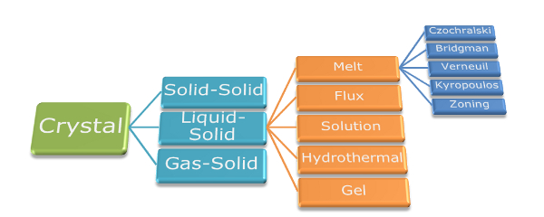
Crystal growth refers to the artificial synthesis of crystals and can be roughly classified into three groups, i. e. solid-solid, liquid-solid and gas-solid processes, depending on which phase transition is involved in the crystal formation. Among these three categories, the liquid-solid process is one of the oldest and most widely used techniques, which can be again divided into different subgroups according to the process medium. Crystal growth from the melt is undoubtedly the most popular method for growing single crystals at large scale. More than half of the technological crystals are nowadays obtained by this technique, including elemental semiconductors, metals, oxides, halogenides, and chalcogenides. source
The advantages of the MBE technique compared to other sediment techniques are that it is capable of growing crystals with a sufficient floor of dirt at a minimum below the 10 ppb level, low crystal growth rates, and low sediment temperatures.
All these advantages make MBE technology the preferred technique for crystalline growth in basic research, such as studying the properties of electrical, optical and magnetic materials.
The MBE technique can be utilized to produce various advanced devices such as high-speed transistors, spin transistors, magnetic semiconductors, superconductors, solar cells, MEMS/NEMS devices, artificial membranes and optoelectronic devices.
This tool is somewhat less popular among researchers because it involves expensive costs, a time-consuming preparation process and requires high skills to handle it. This is because to obtain an epitaxial atomic growth, the growing chamber must be in a very high vacuum of about 10-10 Torr (by comparison, the pressure in space in a 10-12 Torr environment).
However, this tool is easy to handle if we have an understanding of vacuum technology. The pleasure of controlling this tool can be felt when we can see for ourselves the arrangement of atoms of each layer during the growth process and can see the beautiful arrangement of atoms through an electron microscope.
Recently, through fundamental research using MBE, it was manufactured a magnetic semiconductor device based on Gallium Arsenide (GaAs) without involving the mixing of magnetic elements.
In other words, magnetic phenomena have been successfully recorded through semiconductor materials grown through the MBE process without involving the mixing of magnetic elements such as Mn, Co, and Cr.
Usually, the magnetic properties of the material can be obtained from heavy elements of conductors and have no rotation in sub-orbital such as Fe, Co, and Ni. This phenomenon occurs because the distance between the electrons in the d orbital is so close that the electrons can rotate to interact with each other and exhibit magnetic phenomena.
Semiconductor devices are electronic components that exploit the electronic properties of semiconductor materials, principally silicon, germanium, and gallium arsenide, as well as organic semiconductors. Semiconductor devices have replaced thermionic devices (vacuum tubes) in most applications. They use electronic conduction in the solid state as opposed to the gaseous state or thermionic emission in a high vacuum. Semiconductor devices are manufactured both as single discrete devices and as integrated circuits (ICs), which consist of a number—from a few (as low as two) to billions—of devices manufactured and interconnected on a single semiconductor substrate, or wafer. source
Perhaps one wonders how the same phenomenon can happen to semiconductor materials such as GaAs that do not directly mix magnetic elements? Furthermore, this semiconductor material consists of light elements which have only spin electrons in s and p orbital only where the distance between the spin electrons in this orbitals is farther away than the d orbitals to interact with each other.
Through this MBE method, the growth of GaAs at low temperatures with non-magnetic elements of beryllium which are the recipients of the electron surplus from Arsenic
Thus arsenic atoms have a spin surplus that does not have a large number of pairs, close to the number of rounds found on a magnetic element. At this time, the magnetic phenomenon of this non-magnetic material can be seen only at low temperatures.
Conclusion
From the above, it can be concluded that the optimization of the growth method, there is a possibility of a moment this phenomenon will be seen at high temperatures.
If the same method can be used for Silicon, it is not impossible that this so-called spintronics field will shake the electronics industry where the conductivity of the material can be modulated not only through the electric field but also through the magnetic field.
REFERENCE
Clean substrate surface source
Molecular beam epitaxy source
Crystal growth refers to the artificial synthesis of crystals source
Semiconductor devices source


wow, amazing. physics remains one of my favorite subject. and I had readout all these things in 12th grade. as I came across your article, so I remind all those things once again. THANKS alot for sharing it is really interesting.
Wow... @yoes very big engine... It's must a special engine usong for. I like to read but I am not an engineer so I just understand the general explain of your writing. Keep it up bro. Your blog was followed by me. Stay connect and became the best engineer writer... Good luck.