Welcome to this exciting series of everyday electronics where I get you very close to electronics components, their use and how to recognize them and I will be giving out 3sbd each to the first two persons that will provide the answer to the two circuit problems I will provide at the end of this post, do read with interest.
Darlington pair is a name given to two transistors connected in such away as to act like a single transistor. The collector of two bipolar junction transistors are connected together such that the same collector current flows into the two transistors, the emitter of the first transistor is connected to the base of the second transistor making the setup appear to be a single transistor. To understand and appreciate these concepts, let us take a closer look at bipolar junction transistors.
Bipolar Junction Transistors
There are no electronics without transistors which also means that there is no computer without the transistor. Unlike the resistors that are basically two terminal devices, the transistor is a three-terminal device. It is also a semiconductor device in the sense that it has the ability to allow or block the passage of electron. Transistors are broadly divided in two; the bipolar junction transistors (BJT) and the field effect transistor (FET).
The BJT is further divided into two, the PNP and the NPN transistor. This defines the three doped regions of the transistor, the positive (P) and the negative (N) regions. Doping simply means the introduction of certain impurity to a pure semiconductor in order to affect its behavior electrically. These three terminals are the Emitter (E), the Base (B) and the Collector (C). The symbol of NPN is shown right with the arrow pointing outwards from the emitter region while the symbol of the PNP transistor is shown on the right with the arrow pointing inwards at the base.
The transistor plays two major roles in its circuit; switching role in digital circuits or amplification role in an analog circuit. The emitter has the highest weight of doping followed by the base which is fairly doped, hence electron moves from the emitter to the base then to the collector (which is where its name comes from).

))
credit: @henrychidiebere
The schematic of a BJT is shown on the left for NPN and PNP. For the PNP, point A represents the collector-base junction while point B represents the emitter-base junction. For NPN, point D represents the collector-base junction while point E represents emitter-base junction.
Biasing the BJT
From the figure shown above, the BJT has two possible biasing technique, either it is forward biased or it is reverse biased which makes the transistor operate in four possible states.

))
credit: @henrychidiebere
As already stated above, the emitter is highly doped compared to base and the collector, the electron released into the base from the emitter shows up as the emitter current, hence the same amount of electron release at the base also shows up at the collector as a result of emitter influence. With this, it is safe to say that the current at the collector is related to the current at the emitter as a result of voltage at the base-emitter junction.
To summarize the above statement, the principle behind the BJT is the ability to control the current at one terminal by controlling the voltage at the remaining two terminals.
From the statement above, the current at the collector and the current at the base are directly proportional, mathematically,
Ic ∝ IB
Removing the proportionality sign,
Ic = βIB ------(eq1)where β is known as the gain of the transistor
Also applying Kirchhoff’s current law of the circuit above,
IE = Ic + IB --------(eq2) substituting the value of Ic into this equation gives
IE = βIB + IB = (β + 1) IB ------(eq3)
The equations above are the basic transistor equations, the rest is derivative of the above equations.
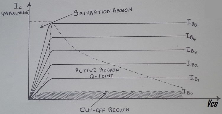
Also as stated above, the transistor is either forward biased or reverse biased, this makes the transistor operate in four regions which are the cut-off region, the saturation region, the active region and lastly the breakdown region.

credit: @henrychidiebere
As shown in the graph above, at the transistor is said to be operating at its saturation region only if the gain β, is greater than the ratio of collector current and base current hence, both base-collector junction and the base-emitter junction are in forward bias. Hence the voltage at the base-emitter Vbe is greater than the voltage at the collector-emitter. What this means is that the transistor allows maximum current to flow through it and offers minimal resistance. In a digital circuit, this region is said to be the “high” state or on state.
At the cut-off region, the base-emitter junction is said to be in reverse bias, hence, no current flows. This is considered the off state. At the active region, the collector-base junction is in reverse bias while the emitter-base junction is in forward bias. Here, the voltage at the collector is greater than the voltage between the collector-emitter junction which in turn is greater than the voltage at the base-emitter junction.
For a transistor to operate as a switch, the saturation region and the cut-off region is enough. But if the BJT is allowed to function in just these two extreme regions, its underutilized. When the transistor is operated in its active region, its collector current is operating between the two extreme regions, the saturation region and the cut-off region.
Finally at the breakdown region, the voltage in the collector region is so large the diode at the base-collector junction loses its semiconductor properties and breaks down thereby allowing excessive current to flow to the collector. This region is undesired as and can be avoided by regulating the collector voltage. With this, we can all understand the concept of darlington pair.
Operation of the darlington pair
The concept of darlington pair is to be able to multiply the gain of two transistor. By so doing, we spend little amount of current to carry out large amount of work (load).
))
credit: @henrychidiebere
Considering the NPN transistors (image A) as stated above, the collector of the first transistor (the master transistor) powers the base of the slave transistor TR2 and hence multiplies the gain of the two transistors. This is because by default, the emitter follower configuration provides very high input impedance (total resistance offered) while providing minimal output impedance hence the amplifier acts as a perfect voltage buffer. Since the same collector current flows through the two transistors, then the collector current is the sum of current in the collectors of the two transistors, mathematically;
Ictotal = Ic1 + Ic2 ------ (eq 4)
From equation 1 above, Ic = βIc, hence
Ictotal = β1IB1 + β2IB2 ---- (eq 5)
But from image (A) IB2 = IE1
Emitter current at TR1 is the summation of TR1 base current (IB) and TR1 current (TR1), hence;
IE1=IB + Ic1 ------ (eq6)
(from eq1) Ic1 = β1IB, substituting into eq6
IE1 = β1IB + IB, making IB the subject, IE1 = (β1 + 1)IB which is also equal to IB2
equation 5 becomes
Ic = β2( β1 + 1)IB + β1IB, expanding the equation
Ic = β2* β1IB + β2IB + β1IB, factoring the gains of the two transistors we have
Ic = (β2 β1 + β2 + β1)*IB -------- (eq7)
From equation 7 above, it is obvious that the gains of the transistors β2 and β1 provide a multiplying effect making the darlington transistors act as a single high gain transistor.
Example:
Two transistors are connected in darlington pair configuration and used to drive a relay of rating 30watts and 10volts. If the gain of the master and the slave transistor are 20 and 60 respectively, find the base current required to bias the transistor.
The common collector current Ic flows to the relay and is given as the ratio of the power to the voltage, hence
Ic = P/V = 30/10 = 3amps; the two gains are β1 = 20 and β2 = 60 hence from equation 7 Ic is given as
Ic = (β2* β1 + β2 + β1)IB, making IB the subject we have
IB = Ic/(β2 β1 + β2 + β1) = 3/(20*60 + 20 +60) = 3/1280 = 0.00234amps = 2.3mAmps
The base current is smaller than the output current Ic though this would have been better if the gain of the master transistor is as high as the gain of the slave transistor.
Application
Darlington transistors are applied in systems requiring low frequency and as already stated, high gain. They are applied in touch sensor technology. Remember the Nokia 5800 expressmusic phones? Their touchscreenswere constructed using the resistive touch technology which was later replaced by now capacitive touch sensors because of its poor responsiveness. Here the tiny voltage induced by the finger is large enough to bias the base of the darlington transistor available in the display ICs.
Darlington transistors are also applied in the voltage regulation and also in microcontroller circuits. They are also used as motor and solenoid drivers.
The SBD...
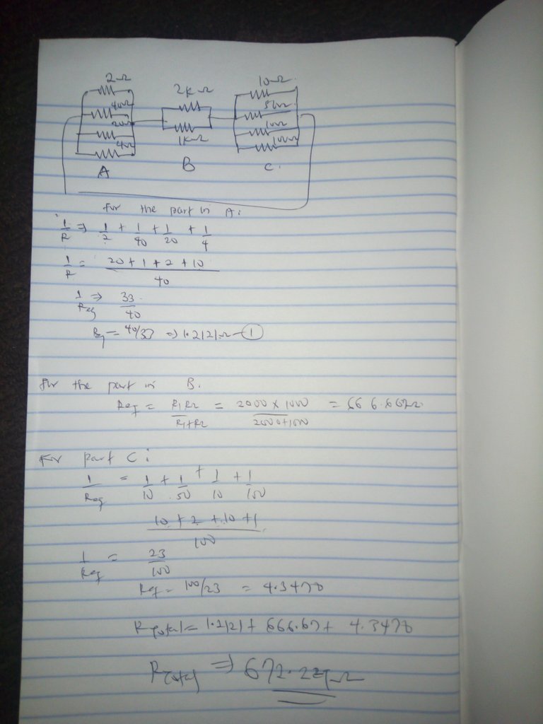
As stated at the beginning of this post, I will be giving 3 sbd each to the first answers to these two questions. No one is allowed to answer more than two questions. From the part #1 of this series I explained different resistor arrangements, hence the first question (Q1)
))
credit: @henrychidiebere
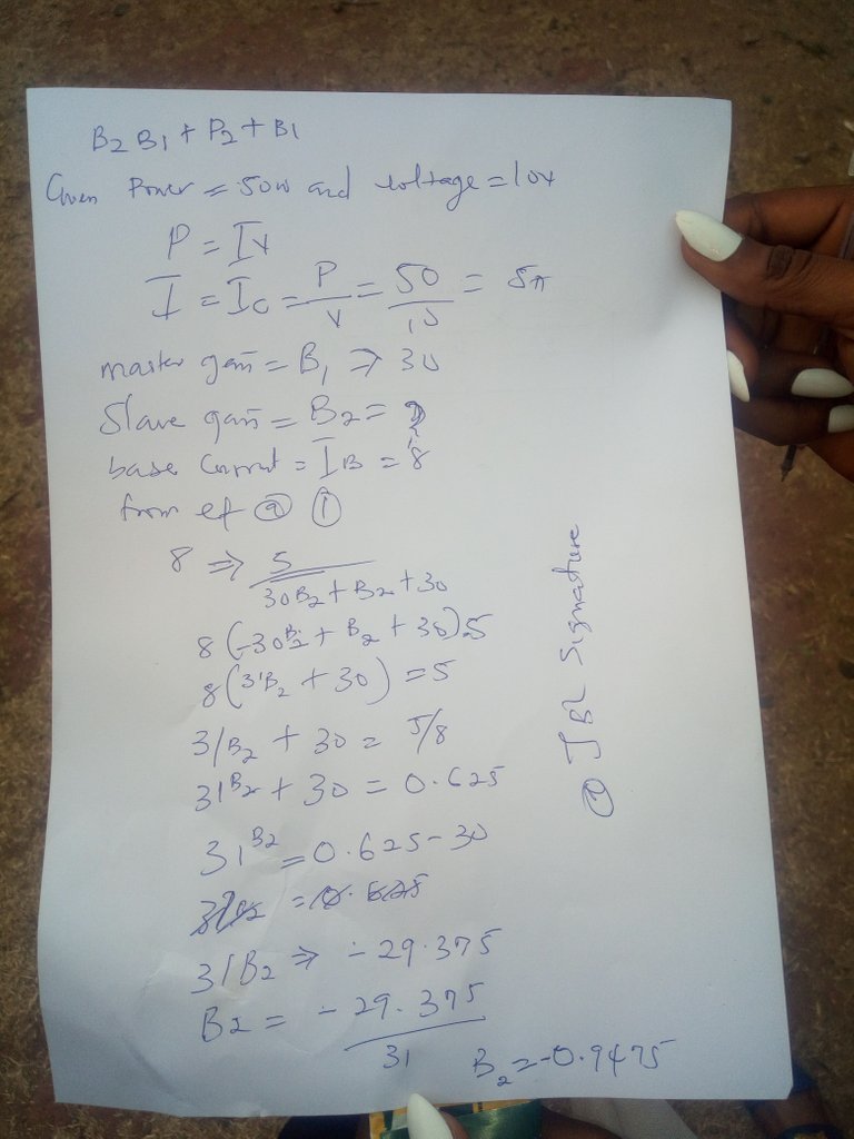
Question 2, Two transistors are connected in darlington pair configuration and used to drive a solenoid of rating 50watts and 10volts. If the gain the master transistor is 30, find the gain of the slave transistor given that the current flowing to the solenoid is 8amps.
Reference
- Darlington transistors -wikipedia
- darlington transistors-electronics tutorial
- emitter follower -electronics notes
- Touch sensor overview -hackaday
If you write STEM (Science, Technology, Engineering, and Mathematics) related posts, consider joining #steemSTEM on steemit chat or discord here. If you are from Nigeria, you may want to include the #stemng tag in your post. You can visit this blog by @stemng for more details. You can also check this blog post by @steemstem here and this guidelines here for help on how to be a member of @steemstem.


))

))
))
))
Being A SteemStem Member
Congratulations @henrychidiebere! You have completed some achievement on Steemit and have been rewarded with new badge(s) :
Click on any badge to view your own Board of Honor on SteemitBoard.
For more information about SteemitBoard, click here
If you no longer want to receive notifications, reply to this comment with the word
STOPFor the first question:
R(equivalent) = 672.229 0hms
correct, sent 3sbd your way
Thanks for your effort, man. God bless you!
Here is the answer to the second question.

3sbd coming your way
thank you for the valuable information
A clear effort
.
you went against the rule bro, delete this comment
So sorry, boss!
BUT: no one is allowed to answer more than two questions
Number 2:
Slave gain = -0.9475
No working
Network ish
SBD received, thank you so much, God bless you
I first u answer tho
u no show working at first....smiles...😀